
Hits:1984 times
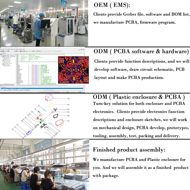
Most PCBA factories only accept clients Geber files and BOM list, then manufacture PCBA. A part of them call PCB layout as designing or developing. When there is any unreasonable designs in your files, they cannot detect it, let alone to improve it for you. In this case, you will find the finished product defective rate is high, or assemly efficiency is very slow when you are assemle the PCBA into the plastic or metal enclosure.
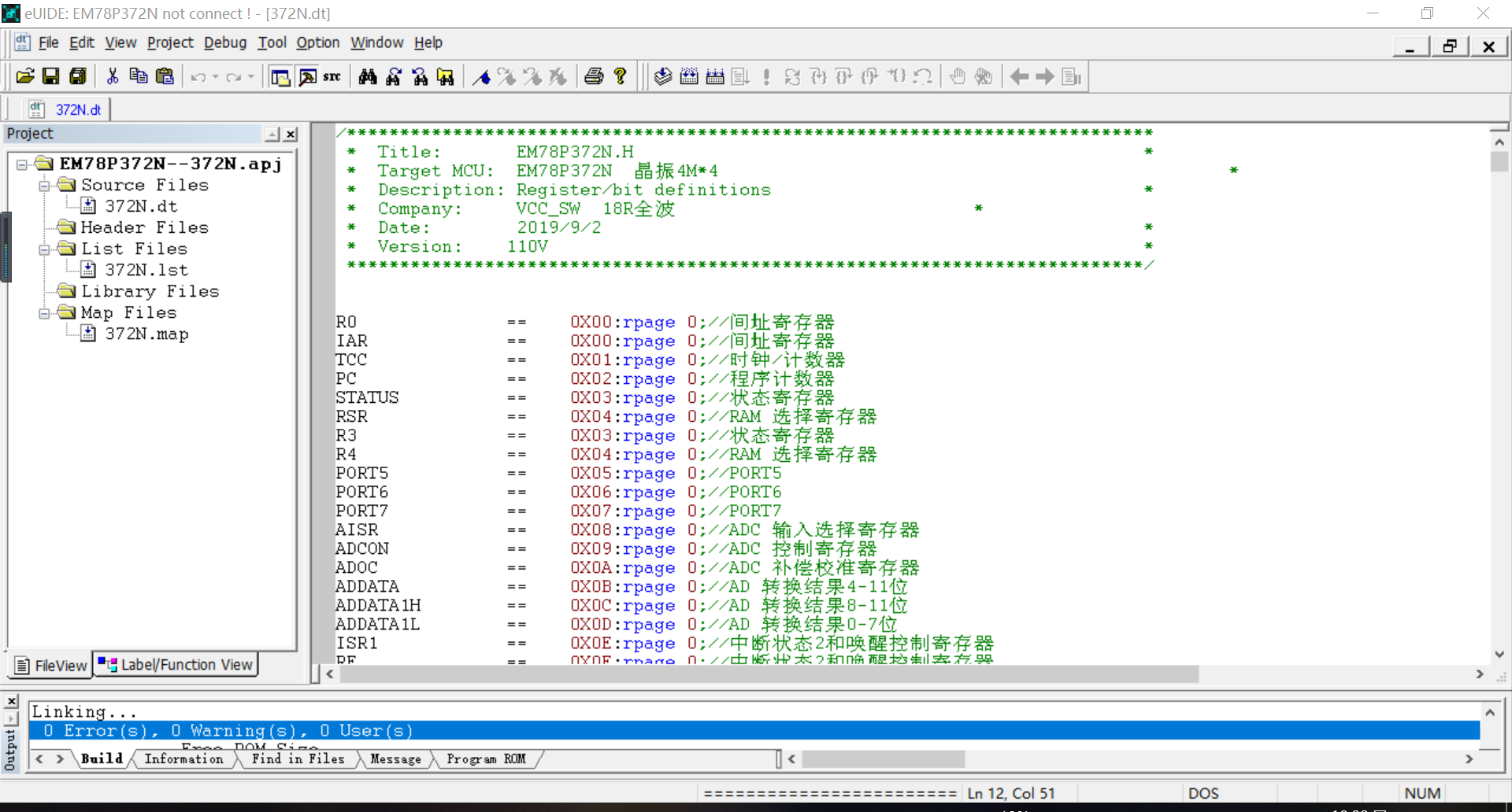
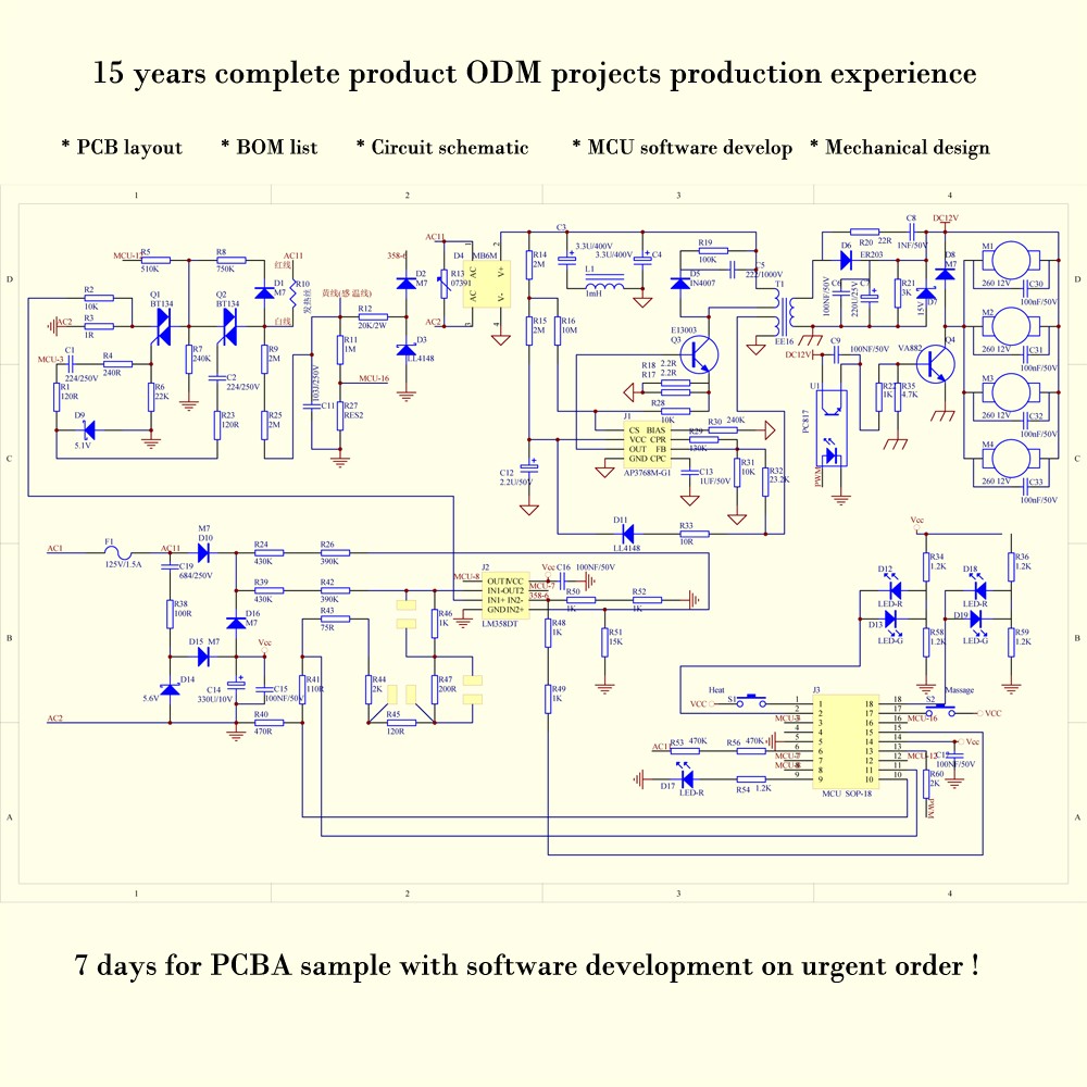
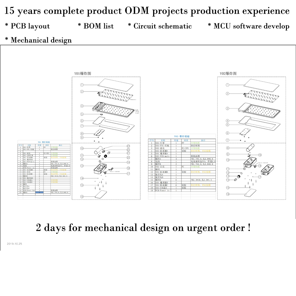
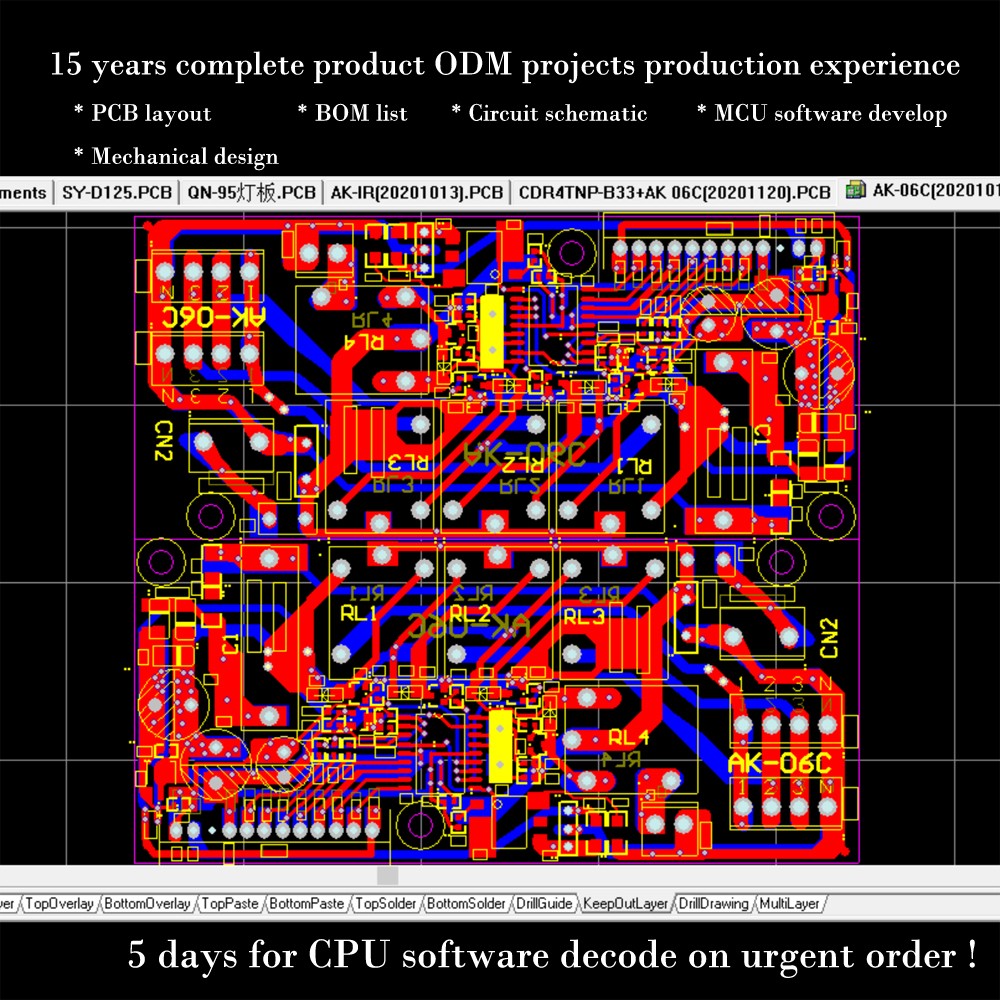
For Shenzhen Soffa, we originally work on ODM finished products including mechanical design for plastic enclosure, developing MCU software, PCB layout, circuit schematic, 3D prototypes, tooling, plastic injection, PCBA manufacturing, enclosure and PCBA assembly, packaging, shipping to overseas. We expericed the whole product developing process since 2006. Therefore, we are very familiar or an expert at making the product. When we receive your files, we will consider the possible defective, production convenience and efficiency, cost economic, etc. Working with us, it will save you a lot of time and money, as well as reduce the produce developing time.
| Product range |
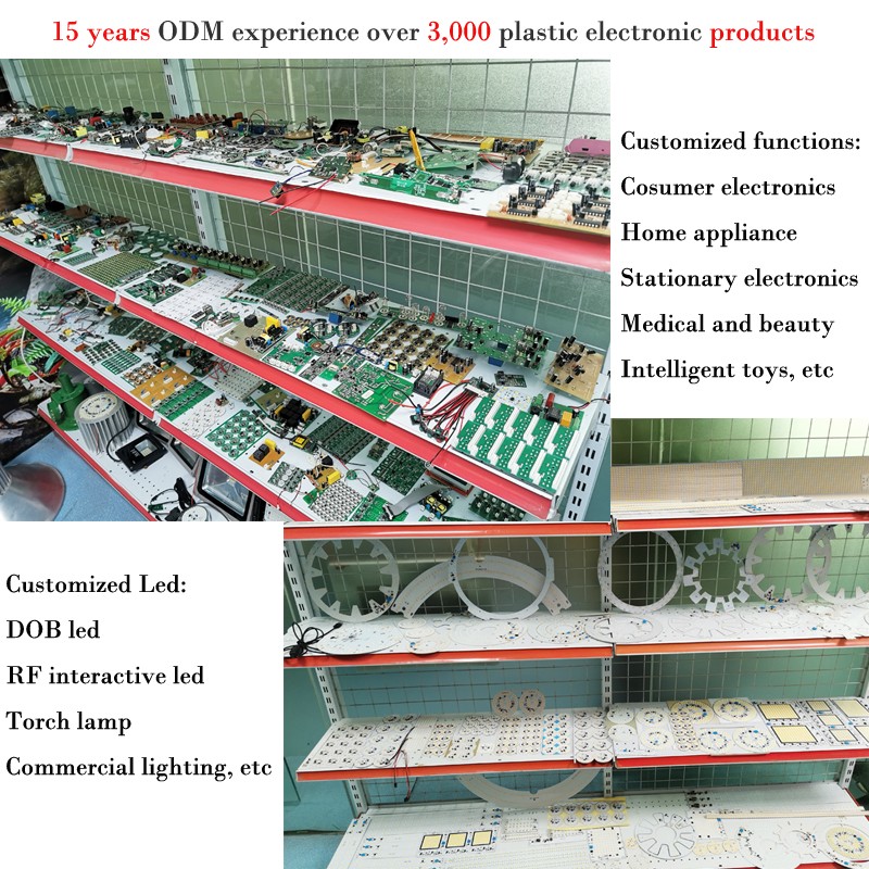
commercial led lighting consumer electronics RF wireless industries interactive led entertainments medical equipment intelligent toys home appliance electronics and other customized products. |
| Design scope |
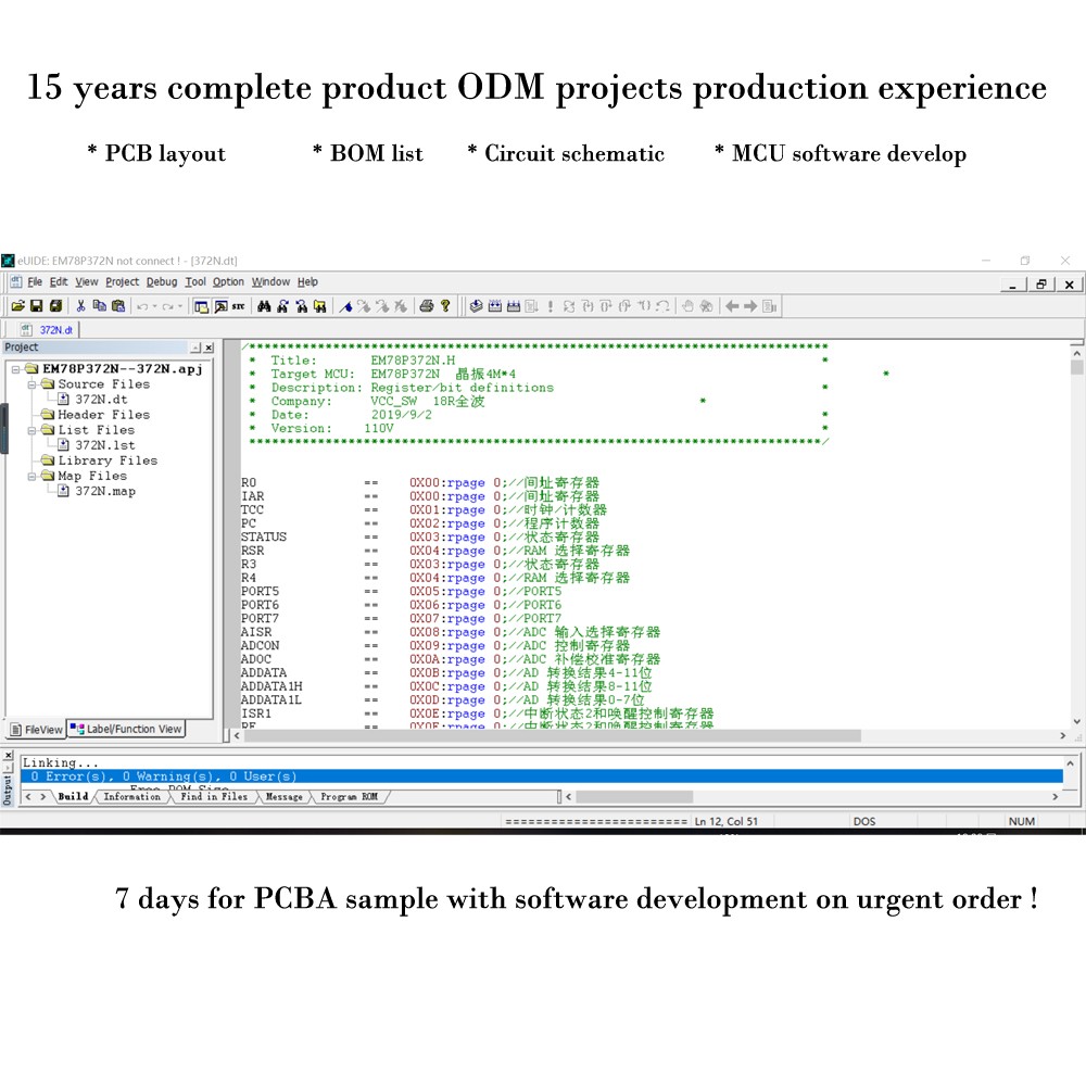
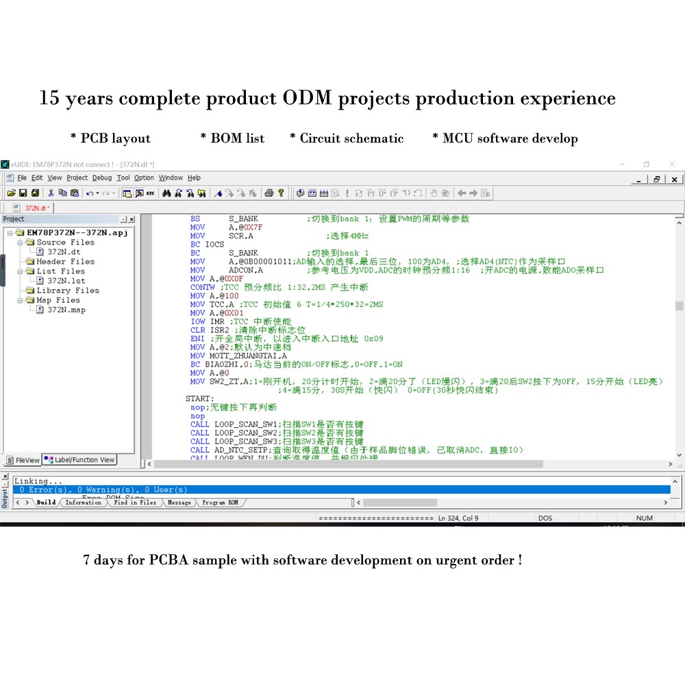
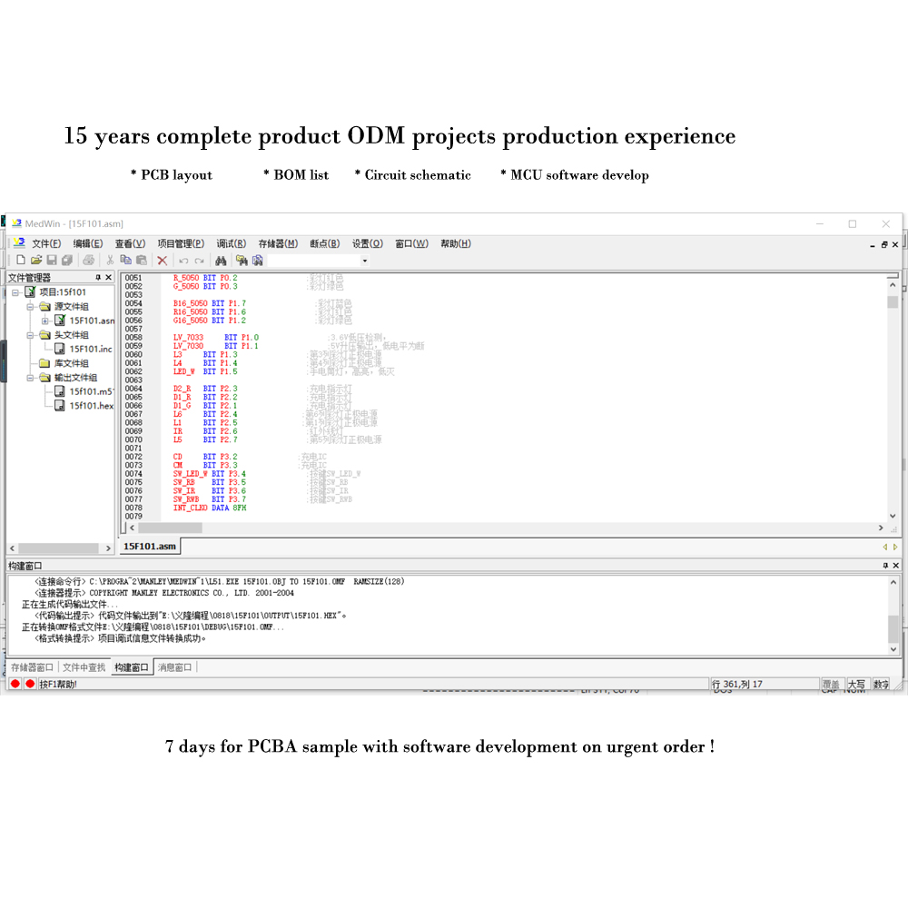
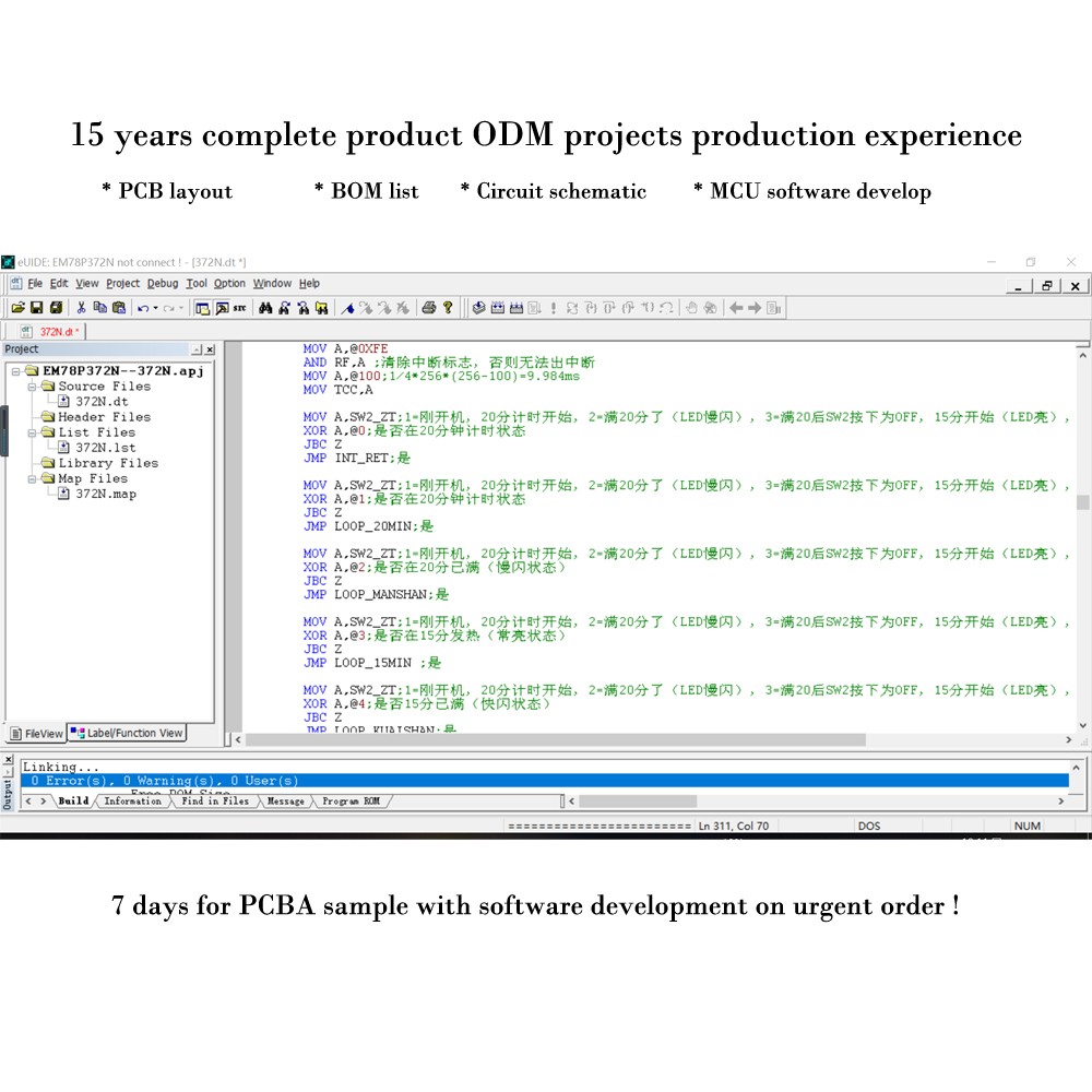
* developing MCU software ( 3~15 days depends on functions ) * PCB layout ( 1 day , or urgently for 3 hours) * circuit schematic ( 1 day , or urgently for 3 hours) * BOM list ( 1 day ) * mechanical design for plastic enclosure( 3 days) * 3D prototypes for plastic enclosure ( 3 days )
|
PCBA prototype lead time | 3 days |
Sample | Free sample available in stocking design or similar functions Sample lead time: 1 day |
Previous:custom pcb design chip on board pcb design pcba pcb layout design
Next:control board clone circuit maker pcb assembly samples pcba reverse engineering service auto clone p